The difference between high-speed optocoupler and ordinary optocoupler in air conditioning
The structure of high-speed optocoupler is different from ordinary optocoupler. The structure of high-speed optocoupler is photodiode + amplifying drive circuit, and the structure of ordinary optocoupler is phototransistor (+amplifying drive circuit). The response speed (rise and fall time) of the photodiode is in the order of nanoseconds, and the response speed (rise and fall time) of the phototransistor is in the order of microseconds. It's not that ordinary optocouplers can work at high speed in the linear region, but their inherent response time is limited. In addition, if the ordinary optocoupler works in the linear region, it will also be limited to the cut-off frequency Fc (Cut-offFrequency) parameter. The Fc of the ordinary optocoupler is basically around 50KHz (test conditions VCC=5v, IC=5ma, RL=100R RL increases and Fc is smaller. When RL=1K, Fc is about 10KHz), like TLP521, Fc is about 50KHz, PC817, Fc is about 80KHz, CNY117, Fc is about 250KHz.
Of course, some ordinary optocouplers can indeed reach a speed of 500KHz when increasing the driving current (to 200MA)/reducing the load resistance (to 500OHM)/optimizing the driving pulse.
Application of high-speed optocoupler
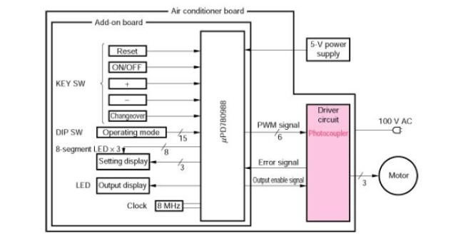
1. High-speed optocouplers are used in air conditioners
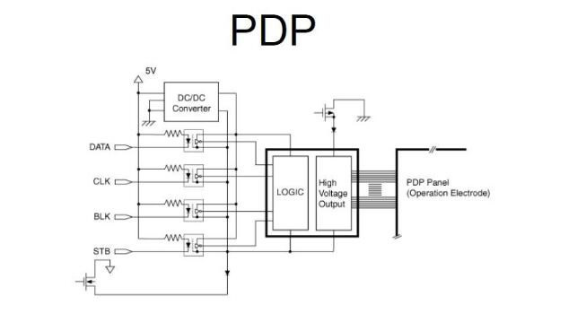
2、High-speed optocoupler used in drive power
The principle and application of high-speed photocoupler 6N137
High-speed photocoupler 6N137 is composed of phosphorous gallium arsenide light-emitting diode and photosensitive integrated detection circuit. The signal is received by the photodiode and amplified by the internal high-gain linear amplifier, and then output by the open collector gate. The 6N137 pin diagram and internal structure diagram are shown in Figure 1 and Figure 2. The high and low level transmission delay time of this photoelectric device is short, the typical value is only 45ns, which is close to the level of the transmission delay time of TTL circuit. With a high-speed performance of 10Mbps, it can fully meet the requirements of an isolated bus in terms of transmission speed. The internal noise protection device provides a typical 10kV/μs common mode rejection function. In addition, 6N137 also has a control terminal, through the control of this terminal, can make the output terminal of the optocoupler present a high impedance state.
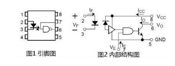
1: NC.; 2: Anode (anode); 3: Cathode (cathode); 4: N.C.; 5: GND; 6: Output (Opencollector open collector); 7: Enable (enable terminal); 8: VCC
The simple principle is shown in Figure 1. If pin 2 is used as input and pin 3 is grounded, the truth table is as listed in Table 2. This is equivalent to the transmission of a NOT gate. If you want to not change the logic state during the transmission, Then input from pin 3 and pin 2 to high level.
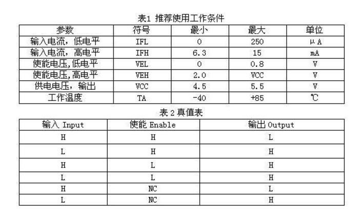
High-speed optocoupler operating conditions
The internal structure principle of 6N137 is shown in Figure 3. The signal is input from pin 2 and pin 3. The light-emitting diode emits light and passes to the photodiode through the on-chip optical channel. The reverse-biased photodiode is turned on after illumination, and the current-voltage After the conversion, it is sent to one input of the AND gate, and the other input of the AND gate is the enable terminal. When the enable terminal is high, the AND gate outputs a high level. After the output transistor is reversed, the photoelectric isolator outputs a low level. When the input signal current is less than the trigger threshold or the enable terminal is low, the output is high, but this logic high is an open collector, and a pull-up resistor or voltage adjustment circuit can be added to the receiving circuit.
The typical application of isolator 6N137 is shown in Figure 3. It is assumed that the input end belongs to module I and the output end belongs to module II. The input terminal has two connection methods, A and B, to get inverted or in-phase logic transmission respectively, where RF is a current-limiting resistor. The forward current of the light-emitting diode is 0-250μA, and the photosensitive tube is not conducting; the forward voltage drop of the light-emitting diode is 1.2-1.7V (typically 1.4V), and the forward current is 6.3-15mA, and the photosensitive tube is conducting. If it is connected by B method, TTL level input, when Vcc is 5V, the RF can be about 500Ω. If the current limiting resistor is not added or the resistance is small, the 6N137 can still work, but the large conduction current of the LED will have a greater impact on Vcc1, especially when the digital waveform is steep, the rising and falling edge of the spectrum is very wide, which will Causes considerable spike noise, and usually the distributed inductance of the printed circuit board makes the ground wire unable to absorb this noise, and its peak-to-peak value can reach more than 100mV, which is enough to make the analog circuit self-excited. Therefore, where possible, RF should be as large as possible.
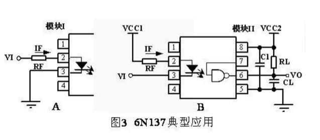
The output terminal is powered by Module II, Vcc2=4.5~5.5V. A 0.1μF capacitor with good high frequency characteristics, such as ceramic dielectric or tantalum capacitor, must be connected between Vcc2 (pin 8) and ground (pin 5), and it should be placed as close to pin 5 and pin 8 as possible (not more than 1cm). This capacitor can absorb the ripple on the power line, and can also reduce the impact on the power supply when the opto-isolator is switched on and off. Pin 7 is the enable terminal. When it is at 0-0.8V, the output is forced to be high (open circuit); when it is at 2.0V-Vcc2, the receiver is allowed to work. See truth table 2.
Pin 6 is an open-collector output terminal, usually with a pull-up resistor RL. Although the absorption circuit can reach 13mA when the output is low, the resistance should still be selected according to the needs of the subsequent input circuit. Because the resistance is too small, the power consumption of the 6N137 will increase, and the impact on the power supply will increase, so that the bypass capacitor cannot absorb it, and interferes with the power supply of the entire module, and even brings peak noise to the ground. Generally, 4.7kΩ can be selected. If the latter stage is a TTL input circuit and there are only 1 to 2 loads, 47kΩ or 15kΩ can also be used. CL is the equivalent capacitance of the output load. It and RL affect the response time of the device. When RL=350Ω and CL=15pF, the response delay is 25-75ns.
